New project to manufacture your own PCB
Creation of new project
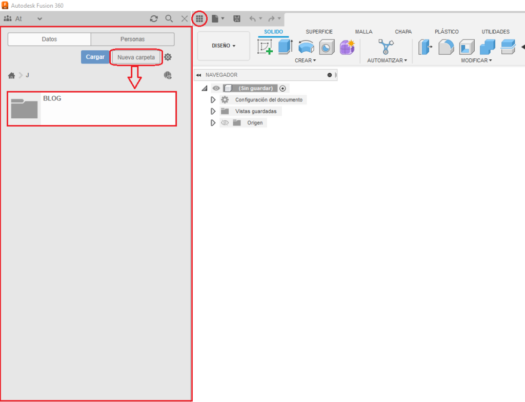
First of all, we recommend creating a folder for the project, even if it is within the same project, in order to have the documents better organized. To do this, click on the New Folder button in the data panel. If you do not see this panel, click on the 3×3 matrix icon at the top left of the Fusion 360 window.
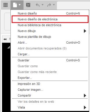
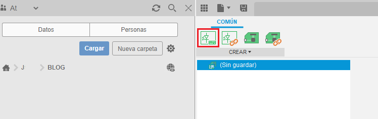
After double clicking on the new folder, we will create a new electronics design and then a new schematic.
Schematic
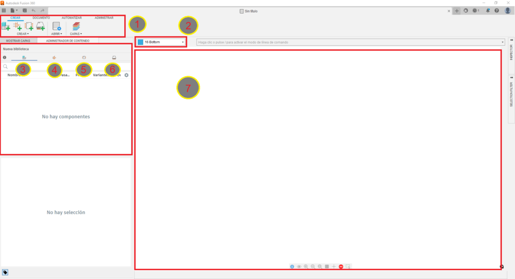
When creating a new schematic, we will be presented with a window like the following one:
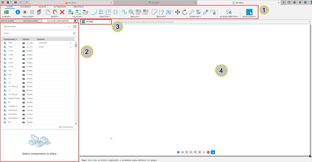
In the upper part (1) we will find the tools with which to design our schematic. It has several tabs to switch between different types of tools.
On the left side of the window (2), there is a panel showing the libraries available for the project, which contain components that will be used to assemble the schematic itself.
Below the design tools (3) we find the layer selector. With this drop-down, we will move between layers to change the layout and include finer details.
Finally, most of the window is occupied by the schematic itself (4), which is where the components will be placed and the connection between them will be made to make sense of our project.
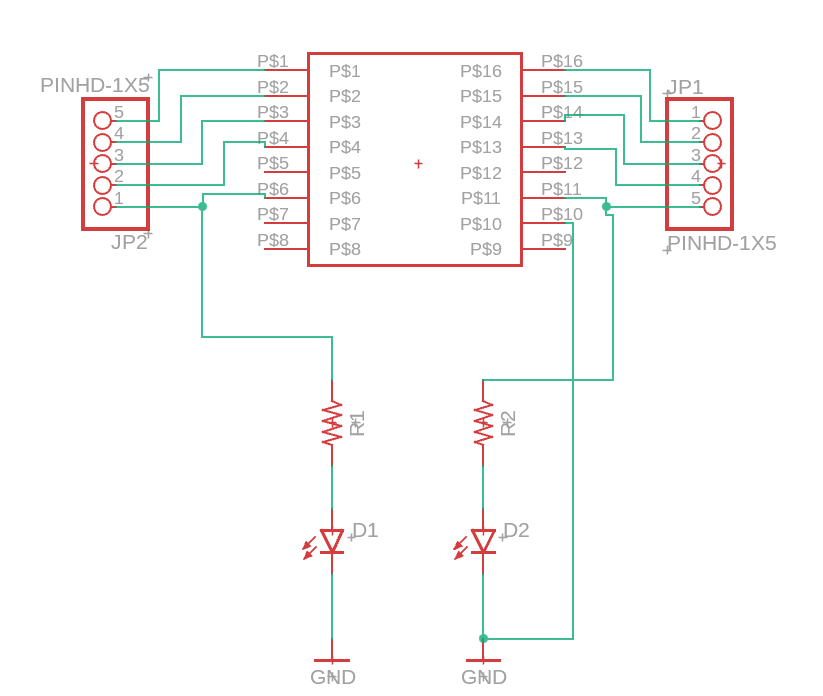
For this example, we are going to create a very simple project involving the use of an ESP8266 type microcontroller, a couple of LEDs and resistors; and a few male pins for general purpose use.
So let’s start by looking for the leds in the library. To do this, we can either scroll through the library panel until we find the led library or search for the word “led” in the search box on the panel.
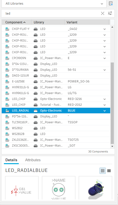
We will choose the component LED_RADIAL from the Opto-Electronic library. The variant can be whatever you want, in this case we have chosen the blue LED. We will place a couple of them in the schematic by double clicking on the component name and automatically the mouse pointer will have the shape of the LED schematic when it passes over the canvas.
Now we will find and place two resistors so that the LEDs can work. As before, search for “resistor” in the search bar.
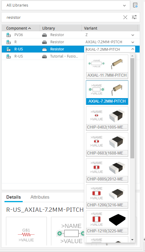
This time, when we choose the variant, we will do it according to the resistors that we physically have, either the 7.2mm long or the 11.7mm long ones. In our case, we will take the 7.2mm ones. The default orientation of this component is horizontal, so if you want to rotate it, right click to rotate it 90 degrees counterclockwise. Once they are in the desired orientation, place them near the LEDs.
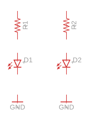
Now we will need to add the circuit ground, where we will connect the cathode of the led diode. To do this, look in the “GND” library. We will choose the GND-BAR component from the Power_Symbols library. When placing it in the schematic, it will ask us to set a value. We will leave the default value of “GND” so that the ground is the same reference throughout the schematic. You can place as many grounds as you want, but in this case we will use only one for the two LEDs.
Now we will incorporate the pins. We will look for “pin” in the library and we will choose the ones from the Connector library. The component will depend on the number of pins, distributed in rows and columns. For example, for a strip of 5 pins in a single row, the component will be named PINHD-1X5. Look carefully before selecting it because, by default, the variant that comes is the one rotated 90º. We will place this component in the desired part of the schematic.
Now it is time to place the ESP8266 microcontroller. By default it is not included in the Fusion 360 libraries so we will learn how to include libraries that we download to our PC.
Include external libraries
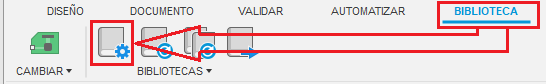
To do this, open the library manager in the “LIBRARY” tab and click on the “Library Manager” button.
Once the library manager window opens, click on the “Import libraries” button and select the option “Import from local disk”.
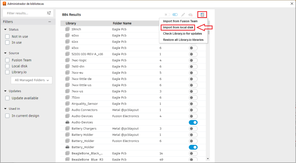
Now all that remains is to browse through folders until you find the lbr extension file that Fusion 360 recognizes as a library.
The ESP8266 library can be found at the following link:
wvanvlaenderen/ESP8266-Eagle_Library: Eagle library for the ESP8266 (github.com)
After importing the library and closing the library manager, we can search for “esp8266” in the library panel and we will see an extensive list:
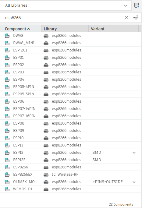
We will choose the WEMOS-D1-MINI component, as it is one of the simplest ESP8266 based boards and has a micro-usb port for connection to a PC.
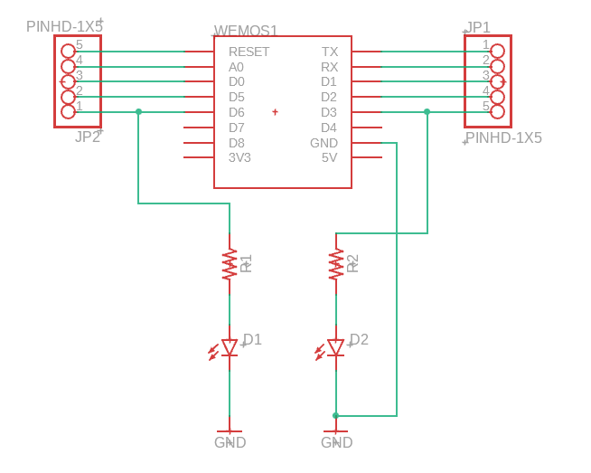
Finally the schematic would be as follows after the incorporation of the microcontroller:
Component connection
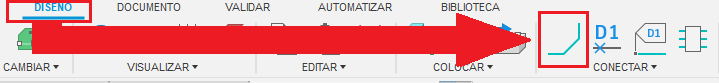
The only thing left to do is to connect components through the Network tool:
With it, we will connect the available points of the electronic components to create a circuit.
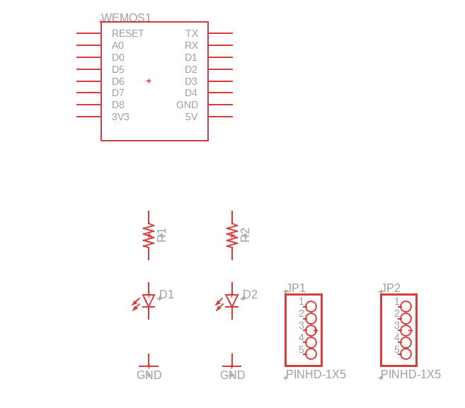
For this example, we have connected one of the LEDs to pin D6 of the WeMos and the other to pin D3. See how it looks in the following image:
Footprint
Once the schematic is finished, with the placement of the components and their connection, it is time to move on to the design part of the “Footprint”. First of all, we will click on the “Change” button and choose the option to “Switch to PCB document”. Or simply go to the next button:

A new tab will open in Fusion360 like the following:
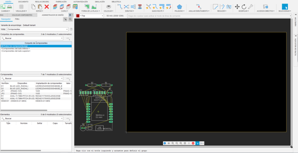
It is time to shape, first, the dimensions of the PCB, and then the distribution of components inside it.
To move the edges of the PCB, use the Move tool in the “Modify” section. We will place the four sides of the rectangle in the desired positions, leaving enough space to place the electronic components.
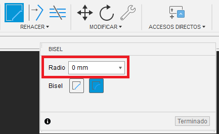
To give a more professional touch to the corners of the PCB, you can use the Round Bevel tool to round the corners:
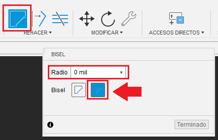
If you look at the image above, the radius is set to 0 mil. What strange unit of measurement is this “mil”? Well, “thousand” is one thousandth of an inch. That is, the result of dividing 2.54 cm by 1000: 0.0254 millimeters. To change these units, we must go to the bottom of this PCB design window:
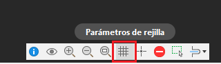
When you click on “Grid parameters”, a window opens for the configuration of these parameters. Normally we work with a grid of 1 millimeter, so in the marked fields in the following image, select “mm” in the drop-down list and in the numeric field enter the value of 1.
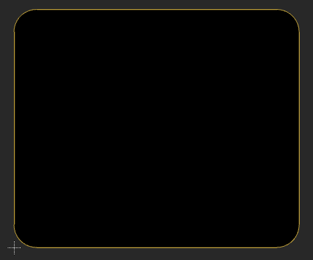
With this, if you go back to the Bevel tool you will see that the unit of the bevel radius has changed. Select or enter the amount you consider necessary and, before finishing, click on the corners of the rectangle so that they are rounded.
This is the result of the plate with a 5mm bevel:
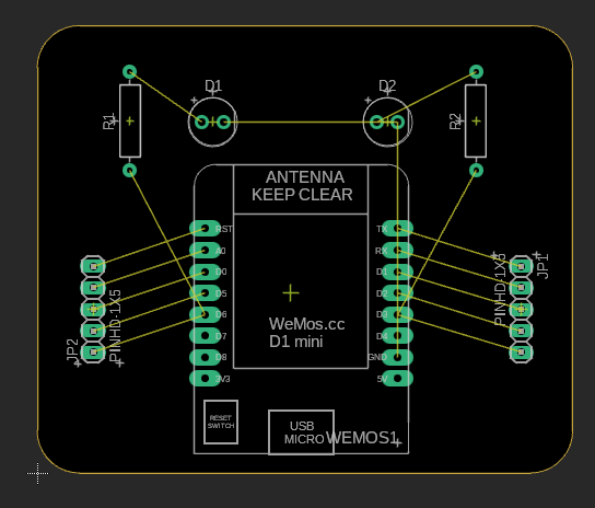
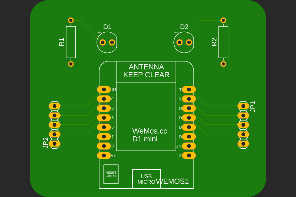
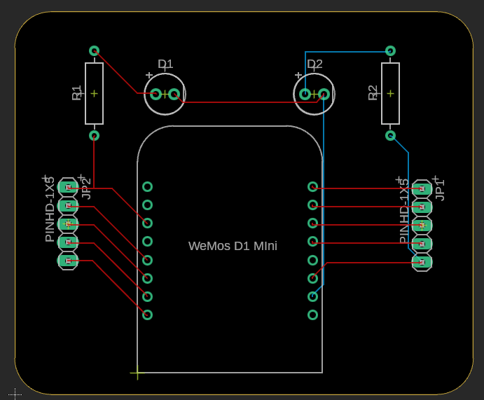
Now we will place the components inside this PCB with the Move tool. You can left click before releasing the components to rotate them 90º. After a homogeneous distribution, the components look like this:
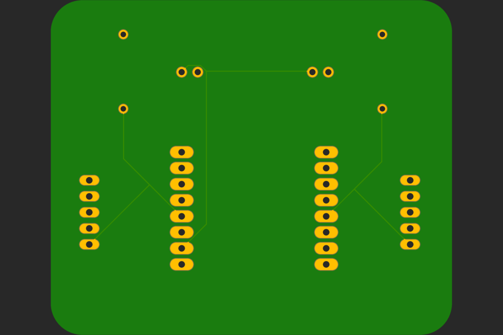
Finally, we only have to “route” the tracks, i.e. connect the components to each other. This task can be done in several ways:
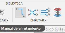
- Manually, with the manual routing tool (It will appear as “Manual routing”, but it is due to its literal translation from English “Manual routing”). As with the “Network” tool in the schematic, we will have to click on the start and end of the route to connect the components.
- Automatically, with the “Automatic Routing” tool. With it you only have to select on which layer you want to route and the program itself will propose a few options (they vary depending on the design) to physically connect components. By clicking on the following button:
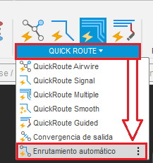
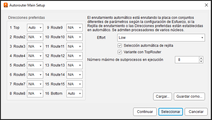
An “Autorouter” configuration window will open. We will leave the default options and click on “Continue”.
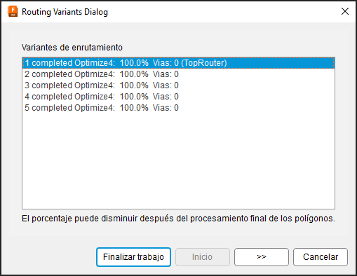
There will be, in our case, 5 routing variants. When you click on the “Start” button, the routing simulation of each variant will start. Select the one you like the most, as long as the percentage is 100% of connected points. Once you have selected one of the variants, click on “Finish work”.
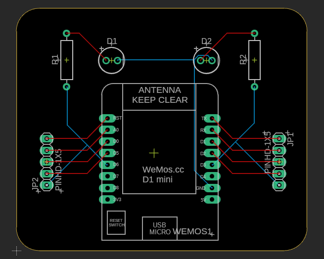
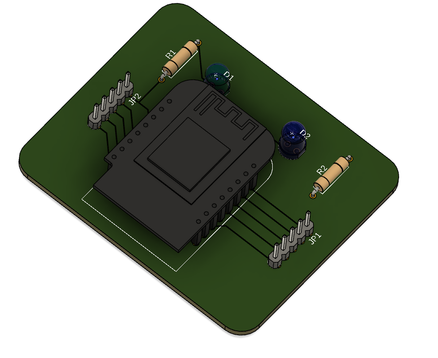
Our design finally looks as follows:
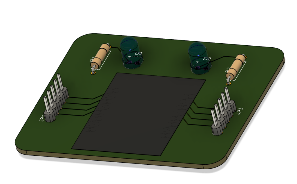
And the PCB image, once printed, will be similar to the following:
Data export
Now that we have our design finished, we need to export the necessary files to send them to the printing company.
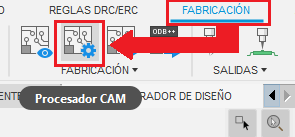
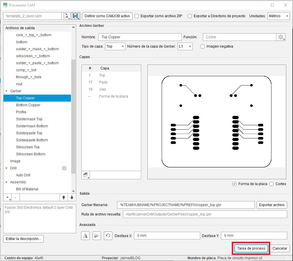
In the “MANUFACTURE” tab of Fusion 360, click on the “CAM Processor” button.
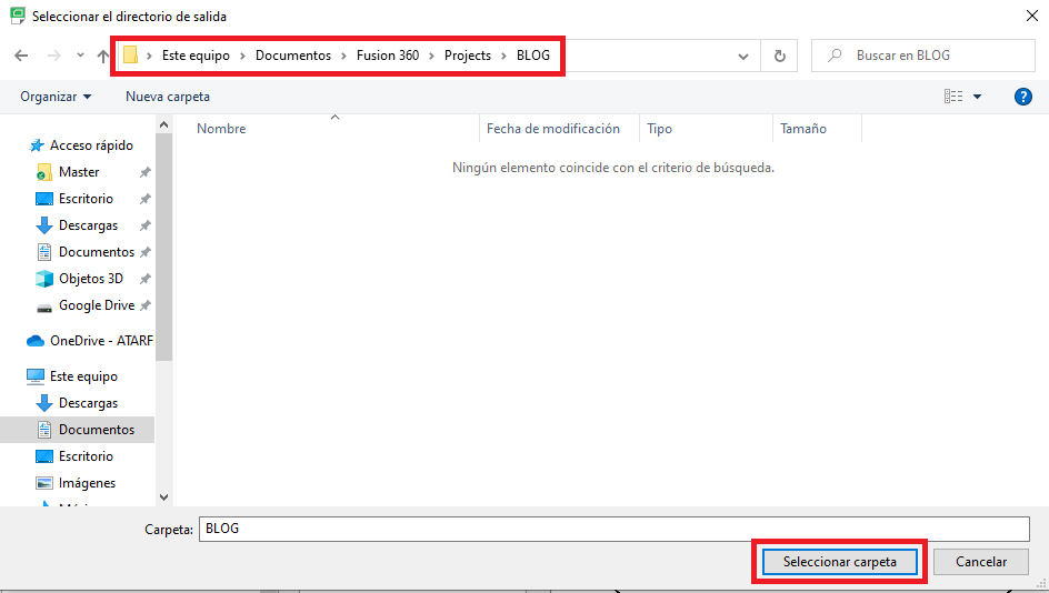
A window will open with several configuration options for exporting CAM files. Normally the default settings are usually left, so just click on the “Process Task” button and choose the folder where the files will be generated.
A new window will open in which you must specify the folder where the files will be exported.
After selecting it, you can open the folder and you should find three other folders organized according to the following names:
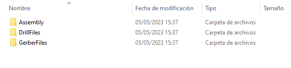
In order for PCB manufacturing companies to understand the design you have just made, you will need to supply them with these three folders compressed into a single file, as these three folders contain all the information that PCB manufacturing machines understand.
Creation of its own library
Whenever you do not find a component on the internet already created in an lbr library, you can create this component yourself thanks to the Datasheet documentation.
Let’s go step by step.
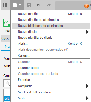
First, you have to create a “New electronics library” via the following button:
A new tab will open like the following one:
In it, there are different parts:
- Tool tab selector
- Layer selector
- Component tab
- Schematic tab
- Footprint tab
- 3D design tab
- Library information panel. Right now it is blank because it is new, but all the designs we create in this library will appear.
In this example, we are going to create our own WeMos D1 Mini, adding a 3D design that we will create ourselves based on the Footprint.
First of all, we must download the Datasheet of this component, including the number of pins and dimensions. Or, if we have one, we will take the measurements and pin spacing ourselves.
Schematic
Once we have the reference documentation, we will start by creating a new schematic. Click on the schematic tab (4) and on the panel that says “No symbols” right click and select “Create new symbol”. We will call it “WEMOS_D1_MINI_SCHEMATIC”, all in capital letters since it does not allow any other option. Adding “SCHEMATIC” or “FOOTPRINT” to the end of these files will help us to avoid errors in the file names.
Entering the name changes the panel (7) a little, adding a design grid. Remember to change it to a 1x1mm grid so that it is compatible with the rest of your projects.
Now we will place a component that has 8 pins at each end, that is, a total of 16. In this part, it is not really important the dimensions that we give to the symbol, but do not make it excessively large since it has to fit in your schematic.
In the “PLACE” tab, choose the “Pole matrix” button. A window will appear in which we can enter the name of the base (which we recommend to leave by default in P$), the pole count (in our case we will write 16) and the initial index of these poles (i.e. the number by which the poles will start to be named), which we will change to 1.
We will be left with a form like the following:
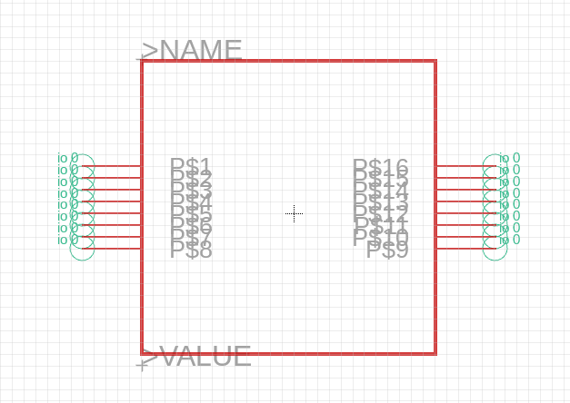
With the Move tool, separate a little the poles of both sides so that the names are not crushed and, if you wish, remove the name of >NAME and >VALUE since they are not needed in this library.
Once the library is aesthetically to our liking, we will save the library and proceed to create the “Footprint”.
Footprint
Now, in the Footprint Tab (5) we will right click and select “Create new component implementation”, which is the same as a Footprint.
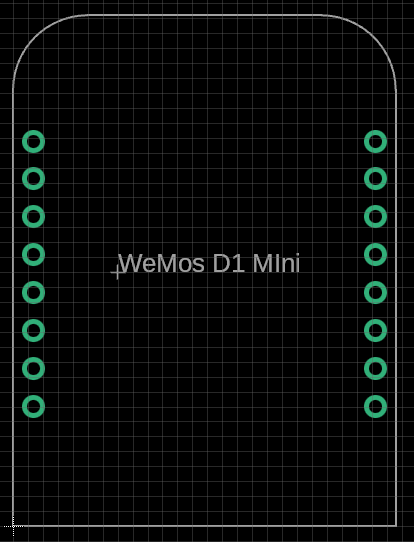
Call it WEMOS_D1_MINI_FOOTPRINT to differentiate it from the schematic. A new window will open with a grid (remember to put it in mm) with a black background. We will have to have the datasheet at hand to capture the same print in this new window, including dimensions and shapes.
In our case we have taken this image for reference:
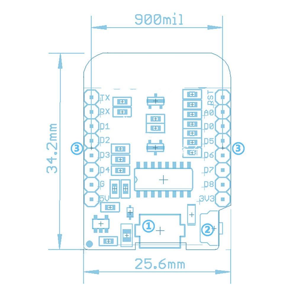
As you can see, the distance between pins is 900mil, which is the same as 22.86 mm (remember that 1 mil is one thousandth of an inch, that is 0.0254mm). We will draw first in layer 21 tPlace the outline of the module:
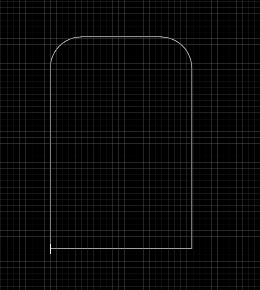
We can adjust the lower right corner more if we want, but we have preferred to leave it like this because this is the space it will occupy including the reset button.
Now we will move on to the PTH pads, which are nothing more than the holes where the module pins will be soldered. To do this, click on the following icon:
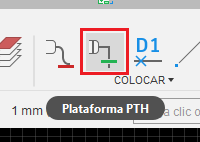
Choose the shape you prefer, either round or square and place 8 holes on each side of the drawing. Don’t worry that they are not well spaced or aligned, now we will put them in place. You should have a footprint similar to this one:
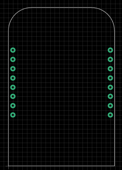
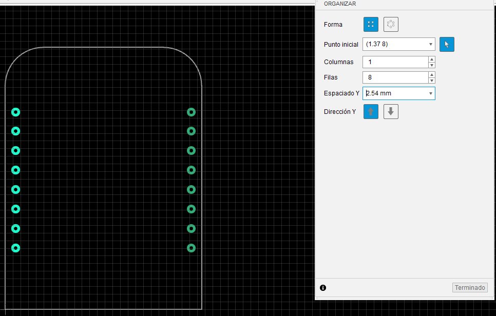
Let’s put the holes in place by selecting all the holes on the left side and, using the “Arrange” tool under the “Modify” tab, place them as follows:
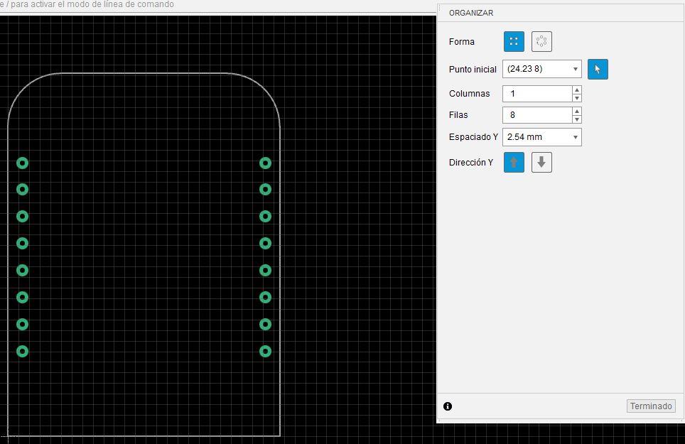
Then, those on the right:
The only thing missing would be to add the name of the module in the middle of the drawing. To do this, we will switch to layer 25 tNames and with the Text tool we will write “WeMos D1 Mini” in the middle of the module. It will look like the following image:
With this we could now save this Footprint and move on to the 3D modeling of this device.
3D Model
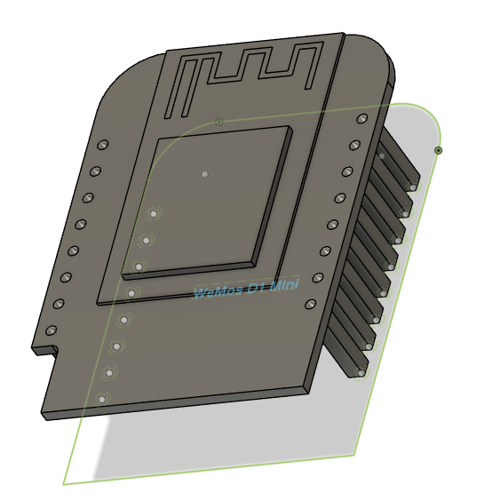
From the same Footprint design window, click on the three dots on the left panel and select “Create new 3D model”.
A new tab will open in Fusion360 for 3D modeling in which we will have the footprint in the XY plane, as a reference. We will name this file “WEMOS_D1_MINI_3DModel”. At this point, we must have some experience in the design of 3D computer parts, either with Autodesk tools, Solidworks, Blender, etc..
Giving free rein to our imagination, although following the original physical model, we will be able to create an object similar to this one:
Finally, save the document and return to the MyLibrary tab to form the Assembly.
Assembly
We will have to go to the components tab to create a new one. Right click and select “Create new component”. We will call it “MY_WEMOSD1MINI”.
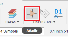
In this new view, we will select the schematic we made earlier from the “Add” button:
We place it in the center of the drawing and now we have to select the Footprint associated to this schematic, the same we have done a few steps back. To do this, in the right panel, in the “New” button, select “Add local package” and we will automatically find the Footprint we have made, which already has the 3D model automatically associated with it.
Finally, we will only have to map the pins of the schematic with the pins of the footprint. To do this, click on the “Connect” button and map each pin with its pad (each pin of the schematic with each pin of the footprint). When they are all, click “OK” to close the window and save the library.
If you want you can test it. To do this, go back to the schematic tab of your main project and let’s replace the WEMOS1 with our newly created WeMosD1 Mini. Find the library in the left panel and place the component.
Be sure to reconnect the previous GPIO and power pins.
Once everything is reconnected, we move on to the PCB layout.
Relaunch the autorouter for a faster track design.
Finally, if we want to see our 3D model with our MeMosD1, just open the view and it will appear automatically:
Wow, what a large understand! I absolutely enjoyed how you approached
this topic — it’s assuredly something I haven’t contemplation not
far from in that way before. Your insights were wonderful engrossing,
and I love how you мейд the whole shebang so relatable.
I can’t wait to charge of more posts like
this! Take care up the awesome work!